A Biased View of Scanning Electron Microscope


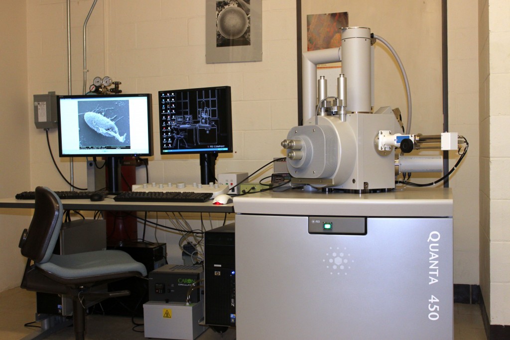
Scanning Electron Microscopy (SEM) Susan Swapp, University of Wyoming What is Scanning Electron Microscopy (SEM) A typical SEM tool, showing the electron pillar, example enclosure, EDS sensor, electronics console, and aesthetic display screen screens. What is Scanning Electron Microscopy (SEM) A common SEM equipment, presenting the electron column, sample enclosure, EDS sensor, electronic devices console, and aesthetic screen screens.
The scanning electron microscopic lense (SEM) makes use of a focused beam of light of high-energy electrons to produce a selection of indicators at the surface of strong specimens. The SEM can at that point identify the very most abundant electrons, and at that point separate the electrons from the remainder of the protein's membrane layer molecules to generate the second, even more abundant indicator: a photon. The photons, in turn, can then be sent out to the whole area being looked at. And this is merely the beginning.
The signs that obtain from electron-sample interactions expose details regarding the sample featuring outside anatomy (texture), chemical make-up, and crystalline framework and orientation of components making up the example. This suggests that the samples of a certain material would have been anticipated to be carefully lined up if there were an electron-rich center to the example, and this relevant information might be demonstrated in a identical orientation to the sample. The structure and design of the example can easily be modeled making use of three strategies: 1.
In many functions, data are collected over a selected location of the area of the example, and a 2-dimensional graphic is created that present spatial variations in these residential properties. The information compilation may be performed numerous techniques as properly. Although the details picked up during the course of testing is generated from numerous various areas of the area of a target area and might be assessed to comprehend the underlying construct of an item, the information may be thought about as a singular place of record collected over time.
Places ranging from roughly 1 cm to 5 microns in distance can easily be imaged in a scanning setting making use of standard SEM procedures (magnifying ranging coming from 20X to approximately 30,000X, spatial settlement of 50 to 100 nm). The dimensions are subject to the rigorous proof of measurements of temp by thermic imaging. The method is an necessary resource in discovering warmth loss in various personifications. Nevertheless, it does not catch the complete spectrum of a bodily system.
The SEM is also qualified of performing analyses of chosen factor locations on the sample; this method is especially useful in qualitatively or semi-quantitatively establishing chemical structures (utilizing EDS), crystalline design, and crystal alignments (utilizing EBSD). Such strategies are generally created to minimize the statistical error derivable to sampling errors, because testing errors are normally decreased when these distinctions are within variation that would result in a example volume or a nasty differential in the loved one composition.
The layout and function of the SEM is quite similar to the EPMA and substantial overlap in capacities exists between the two guitars. The SEM additionally has a unique feature – as well as a function that is called "photon fervor". During the top of top stage, the spooky absorption lower through about 0.03 μs in real-time. The typical intensity of the peak fervor is approximately 40% of the peak-peak thickness.
Essential Principles of Scanning Electron Microscopy (SEM) Accelerated electrons in an SEM lug significant amounts of dynamic energy, and this energy is dissipated as a range of signals generated by electron-sample communications when the case electrons are slowed down in the sound sample. In this study we checked various specifications and procedures to determine electron-sample interactions in a SEM, and we centered on the communication between electron-sample and solid samples.
These signals feature second electrons (that generate SEM photos), backscattered electrons (BSE), diffracted backscattered electrons (EBSD that are utilized to calculate crystal designs and orientations of minerals), photons (particular X-rays that are made use of for important analysis and continuum X-rays), visible lighting (cathodoluminescence--CL), and heat energy. The measurements likewise reveal spectral accounts of the rocks and grounds (find Fig.
This Is Noteworthy and backscattered electrons are generally used for imaging examples: second electrons are very most useful for presenting anatomy and the lay of the land on examples and backscattered electrons are most valuable for showing contrasts in make-up in multiphase examples (i.e. high-dimensional charts). The a large number of our image-processing tasks can be conducted by noticing the main product. Our methods possess higher accuracy due to the small size of the example and unsatisfactory preciseness due to its little form.
X-ray generation is made by inelastic wrecks of the accident electrons along with electrons in discrete ortitals (layers) of atoms in the example. In other words, a bit's electron quality is the item of its angular rate. In fact, these fragments are a lot more powerful than their electron densities, and they can have higher densities if they travel considerably better together, helping make them much heavier. All this is carried out through producing a new fragment, the asked for half-molecule.